

Description
- Operating voltage: 2.4V~5.5V
- Operating current: 4.0mA @5V
- Deep Sleep mode current: 0.5μA @5V
- RX sensitivity (5V, 25℃, BER = 0.1%): -108dBm @10Ksps
- RF operating input power: -108dBm~+10dBm
- Modulation: OOK
- Symbol rate: 0.5Ksps~40Ksps
- Interface: I2C (address: 0x23)
- Dimension: 16 x 15 x 2.6 mm
- Net weight: 1g
The BM2302-6x-2 series offers four operation modes: Deep sleep mode, Auto RX mode, Sniff RX mode, and Configuration mode.
The product automatically enters deep sleep mode after powering on. In deep sleep mode, the power consumption is only 0.5μA. By controlling the DO / SDA and SD / SCL to enter RX mode or configuration mode.
Exit Auto RX mode: power off the module.
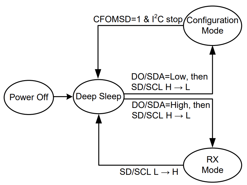
You can select to enter Auto RX mode or Sniff RX mode to receive data.
Auto RX mode
Connect the SD/SCL pin to GND and then power on the module to enter Auto RX mode. The module automatically receives RF signals transmitted from the antenna and outputs the data to the DO / SDA pin after demodulating.
Sniff RX mode
Connect the module’s SD/SCL pins to the MCU to control the voltage level, and use the voltage level to determine whether the module enters the Sniff RX mode.
⬥ When SD / SCL pin is high (powering on the module): enter Deep Sleep mode
⬥ When SD / SCL pin is low: enter Sniff RX mode
In configuration mode, you can configure the internal registers to determine the receiving channel through I2C interface. However, configuration mode is not required for normal operation.
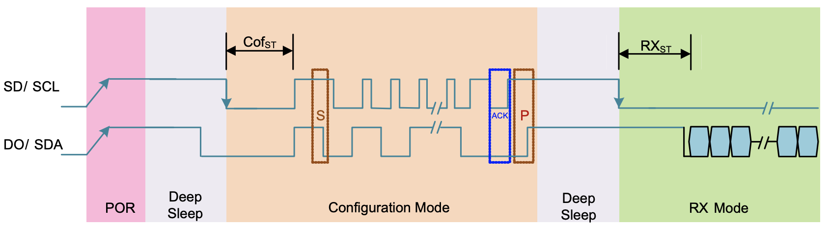
To enter configuration mode, you need to connect both the SD / SCL and DO / SDA pins to the MCU and enter configuration mode after powering on. When the module is in configuration mode, the SD / SCL and DO / SDA pins are used as I2C interface. It can turn back to deep sleep mode by setting the CFOMSD = 1.
The sequence diagram of entering/exiting the configuration mode is as follows:
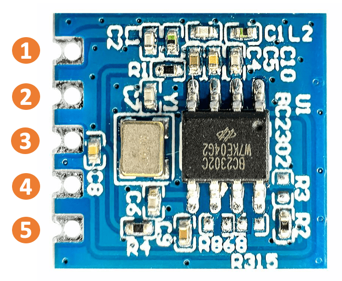
| Pin | Pin name | Function |
|---|---|---|
| 1 | ANT | Antenna interface |
| 2 | GND | Ground |
| 3 | VDD | Power supply: 2.4V~5.5V |
| 4 | DO SDA |
Demodulated data output (RX mode) I2C: data line (configuration mode) |
| 5 | SD SCL |
Exit RX mode: low level I2C: clock line (configuration mode) |
| Function | BM2302-6x-2 | BM2302-6x-1 |
|---|---|---|
| Operating voltage | 2.4V~5.5V | 3.0V~5.5V |
| Operating current | 4.0mA @433MHz | 3.2mA @433MHz |
| Deep sleep mode current | 0.5μA @5V | 0.5μA @5V |
| RX sensitivity (@5V, 25℃, 433MHz) |
-108dBm @10Ksps | -112dBm @10Ksps |
| RF input power (Max.) | +10dBm | +10dBm |
| Frequency band | 315MHz/433MHz/ 868MHz/915MHz |
315MHz/433MHz/ 868MHz/915MHz |
| Modulation | OOK | OOK |
| Symbol rate | 0.5Ksps~40Ksps | 1Ksps~20Ksps |
| Dimension | 16 x 15 x 2.6mm | 16 x 15 x 2.6mm |
- MCU: Holtek BC2302C/D, Sub-1GHz Low-IF OOK RF Receiver, including datasheet, package information, etc.
- Module: BM2302-64-2, Sub-1GHz OOK RX Module.
- Application note:
1. AN0633EN, BC2302C/D Development Board Application Note, including example program
2. AN0631EN, BC2302C/D & BC2302A/B Application Difference Instructions


Reviews
There are no reviews yet.